Weird Science - Tales from the
Vectrex Academy Lab
Vectrex
Project Title
Synopsis
- 64K FRAM PCB Board for the Vectrex cartridge slot
- Freely use up 57.75K of persistent RAM for
programming and for applications
- Easily develop and run custom BIOS versions on the
Vectrex
- Easily flash binary images to any memory address,
either with an EPROM burner, or directly from a PC
over USB cable connection
- Easily use external cartridges with flashed custom
BIOS
Project
Status
- Work in progress
- Fully functional beta version PCB now assembled
and being tested
Motivation
- Some time ago I started experimenting with using a
Hitachi 6309 CPU in the Vectrex and with programming
custom BIOS versions (see here).
I used nes4life's Multi BIOS PCB,
which worked great, but removing the PCB
from the inside of the Vectrex console and
plugging it in again each time I needed to
flash a new version, turned out to be very
cumbersome for BIOS development.
- At some point
in 2023, I talked about this to Andreas
Reber, who is a colleague of mine and an
expert for embedded systems and hardware
design, with a long experience in that
field, reaching back to the days of the
ATARI ST, for which he built several
hardware extensions.
- Together we
came up with ideas and a concept for an
extension cartridge for the Vectrex which
allows for a smooth and easy development of
Vectrex system-software and applications.
This translates to that I told him a long
list of wishes, and he designed and built a
great and powerful toy for me to play around
with: the Vectrex Developer.
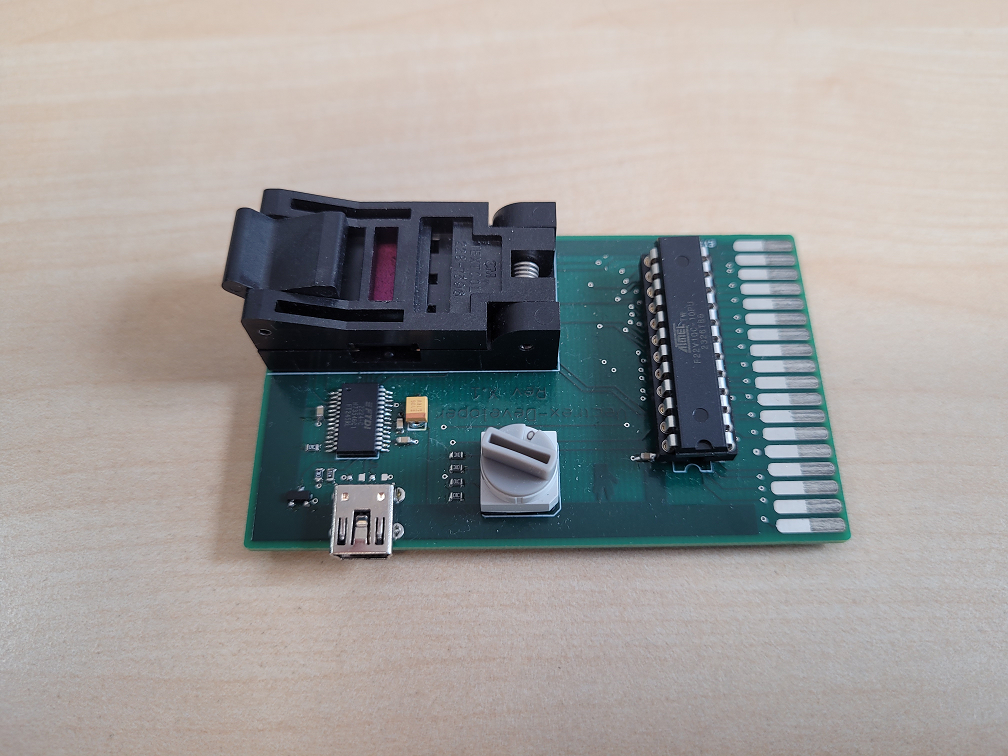
Vectrex
Developer Cartridge
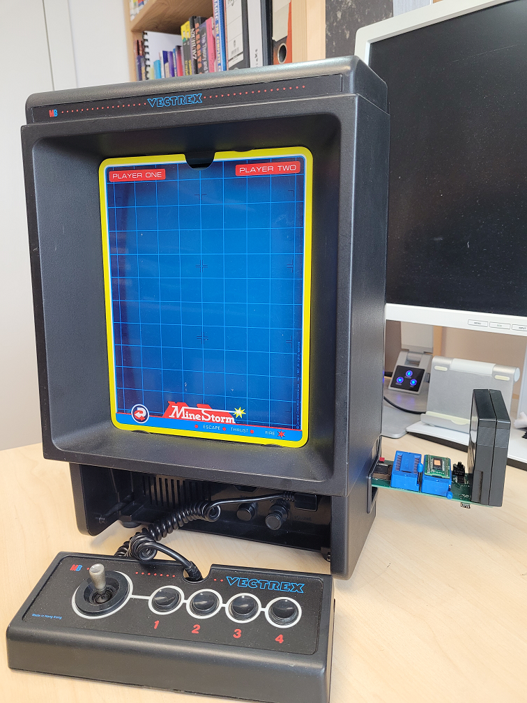
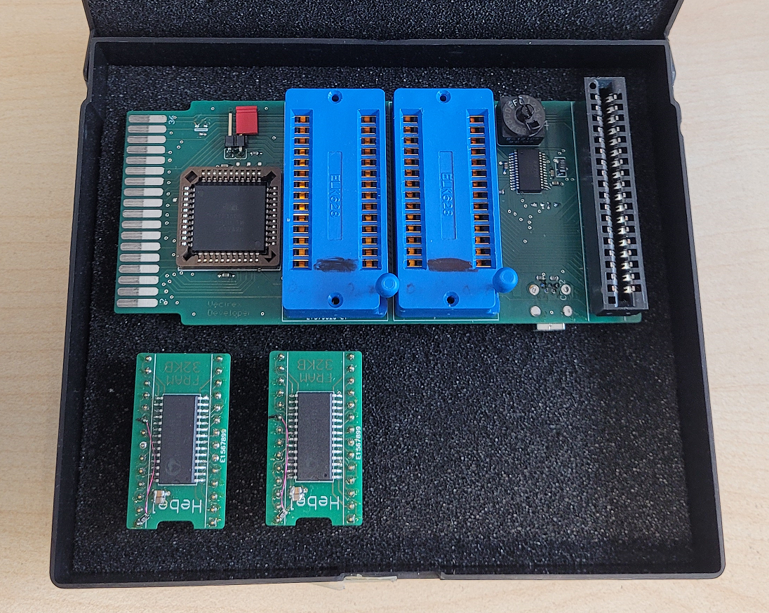
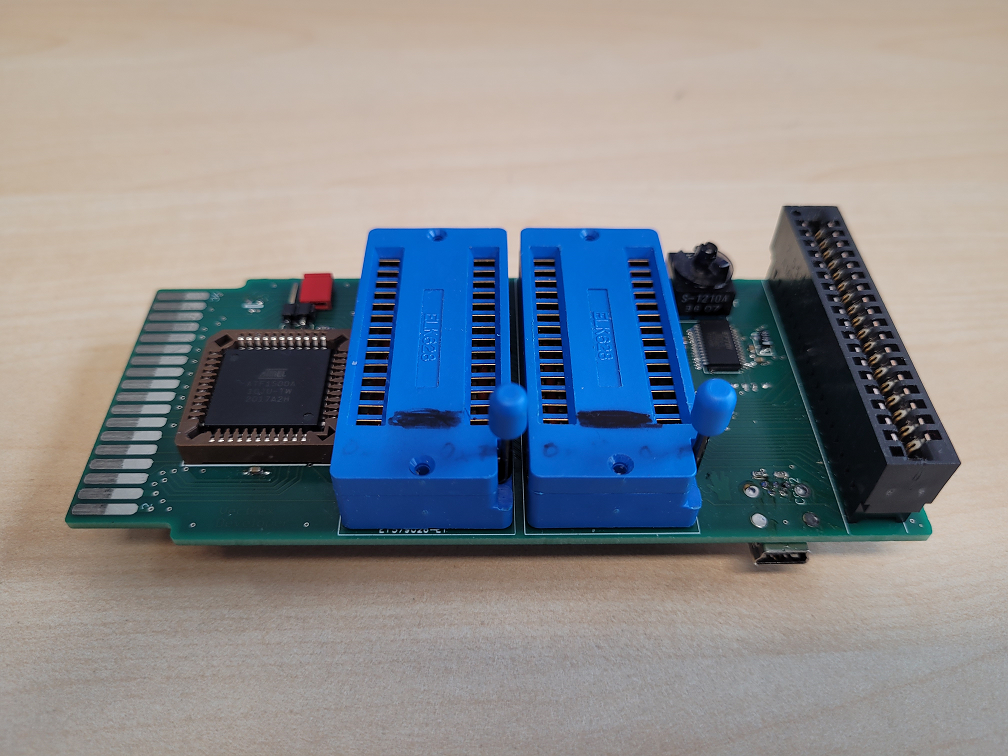
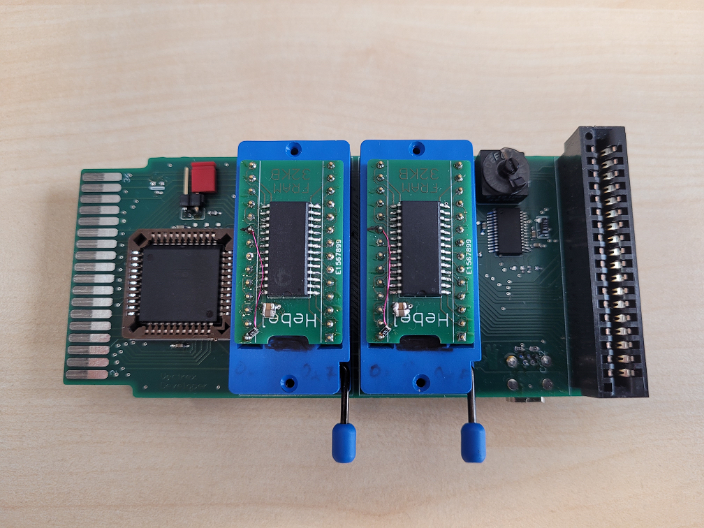
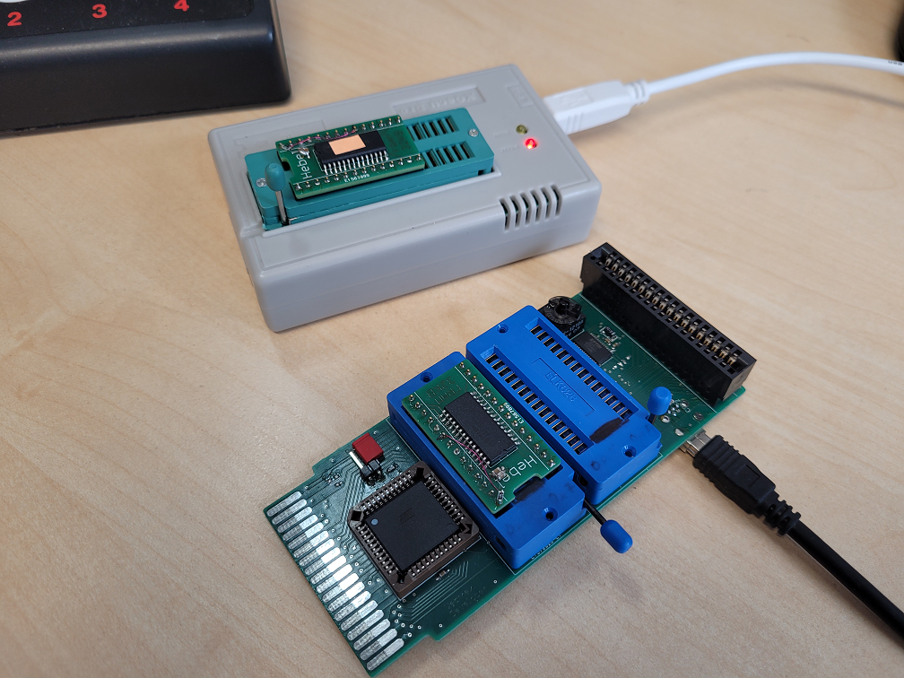
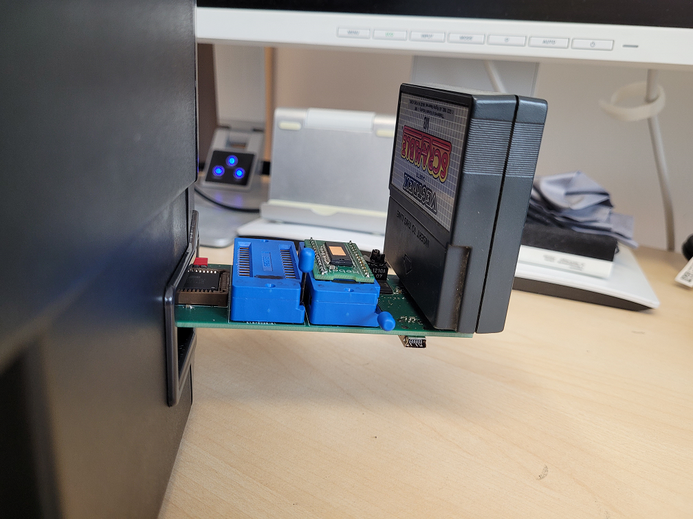
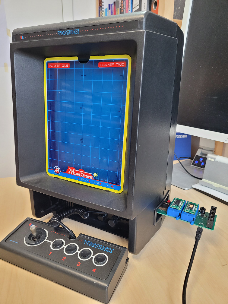
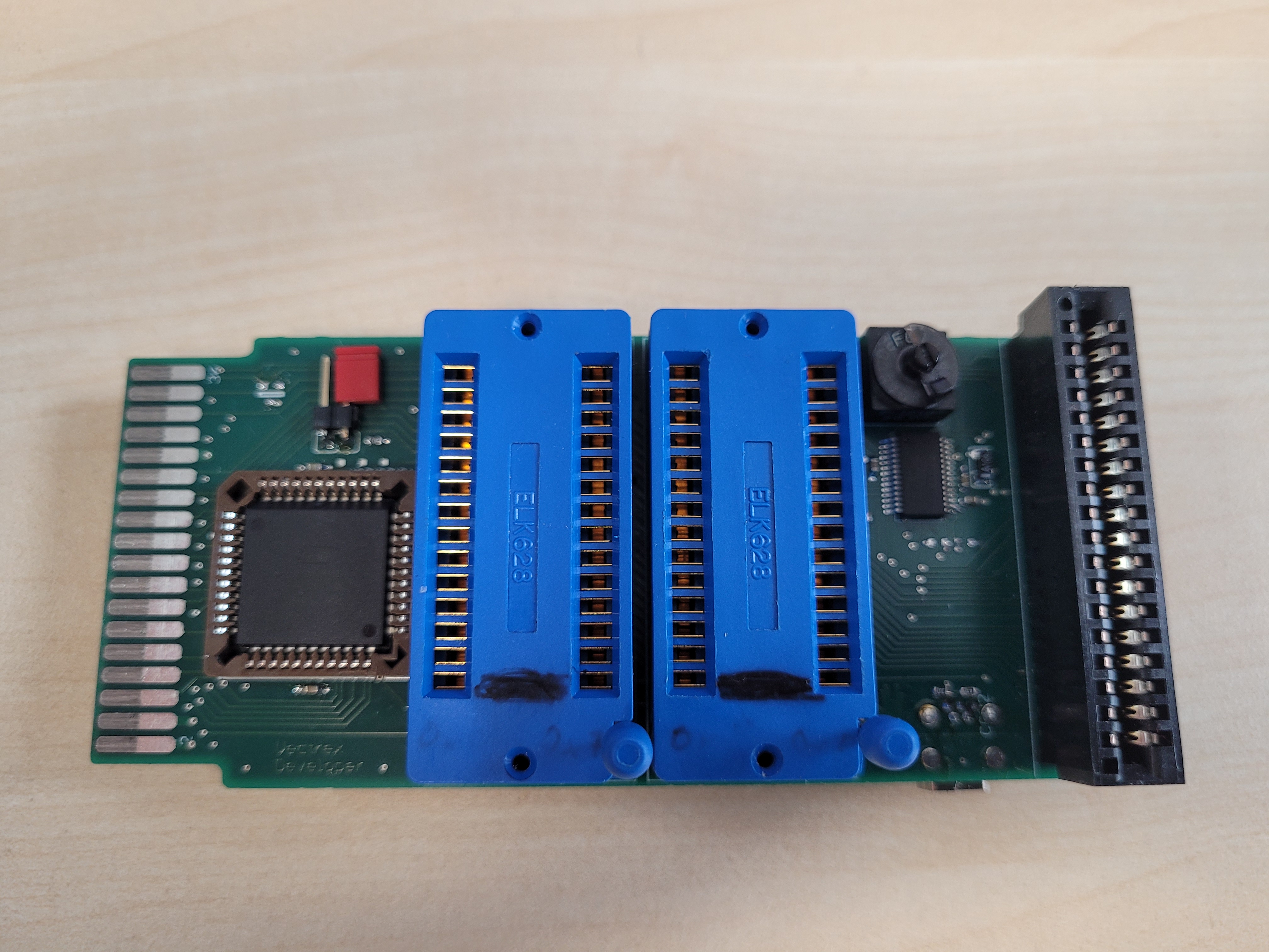
- The Vectrex Developer PCB can be inserted directly
into the Vectrex cartridge slot.
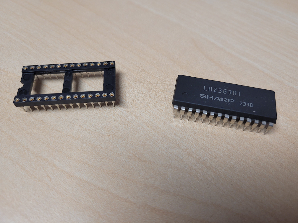
- On the board, there are two ZIF-sockets, each of
which can hold a removable 32K FRAM. An FRAM works
like a Flash-RAM and retains its contents after
power-off.
- The left socket is mapped to the lower 32K of the
Vectrex address space (0x000-0x7fff),
the right socket is mapped to the upper 32K (0x8000-0xffff).
For more on the memory mapping see the respective
section below.
- The board also holds an FTDI UART interface chip,
and a USB cable connector for communication with a
laptop or PC.
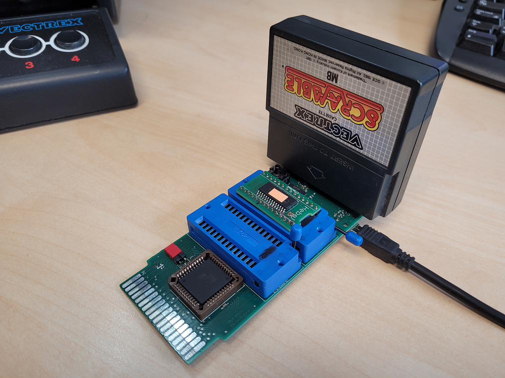
- On the very right side of the board, there is also
an additional external Vectrex cartridge slot.
Technical
Requirements
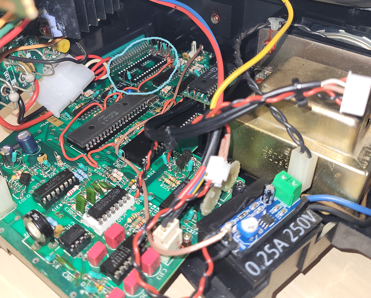
- For the Vectrex Developer cartridge to work, the
internal Vectrex BIOS chip needs to be removed
(unsoldered) from the console's digital board.
- This sounds worse than it actually is. Just remove
the back cover of the Vectrex, and the chip can
easily be unsoldered by working from the bottom-side
of the digital board. There is no further
disassembly of the console necessary.
- It is a good idea to solder in a chip-socket while
being at it. Then the original BIOS chip can easily
be reinserted again at any time, and the console is
restored to its original state.
Vectrex
Memory Space and Memory Mapping
- When the internal BIOS chip is not present, then
the Vectrex CPU will now read the respective BIOS
addresses (0xe000-0xffff) from the
Vectrex cartridge slot, and thus from the Vectrex
Developer cartridge.
- In fact, the Vectrex CPU will now read (and write)
any address from the cartridge slot, except for the
0xd000-0xdfff
range, which is still internally mapped to the VIA,
and for the 0xc800-0xcfff range, which
is still mapped to the internal 1K Vectrex RAM.
- Any other address is routed to the cartridge slot,
meaning that the full range from 0x0000-0xc7fff
and from 0xe000-0xffff is now FRAM,
which amounts to a total of 58K, and which can now
freely be used by the programmer (well almost, the
range from 0xc700-0xc7ff is mapped to
the FTDI UART and reserved for the USB
communication, see section below).
Use Cases
- Plug the Vectrex Developer into the cartridge slot
of the console.
- Flash any BIOS and Mine Storm version you like to
0xe000-0xffff
range of the upper FRAM of the Vectrex Developer.
- Flash any binary you like to the FRAM range of 0x0000-0xc6ff
(~49.75K) and run it with the chosen BIOS.
- Or leave the lower ZIF-socket empty and attach any
cartridge to the external cartridge connector and
then run the cartridge with the chosen BIOS.
- There is no need to remove the Vectrex Developer
from the console's cartridgeslot. Flashing the FRAMs
can be done by removing the chips from the
ZIF-sockets and by using an EPROM burner, or by
leaving them inside the ZIF-sockets and by writing
data to them which is obtained from a laptop or PC
over the UART USB connection.
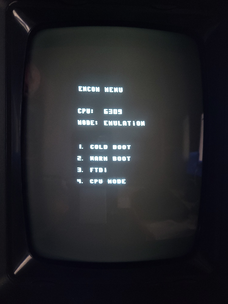
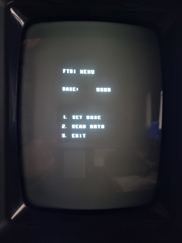
FTDI UART
USB Connection and Boot Loader
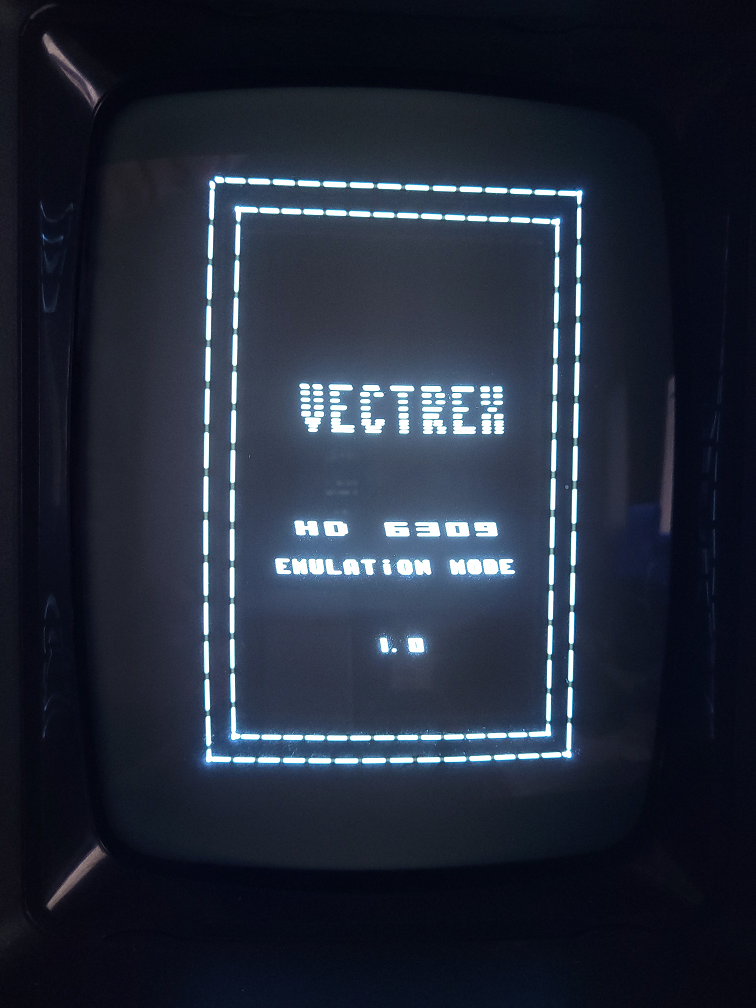
- For the current version of the Vectrex Developer,
I have written a boot loader which is started when
the console boots or resets. In our setting, the
upper FRAM contains the boot loader and three
different BIOS versions (6809, 6309 emulation mode,
6309 native mode).
- The boot loader itself is a regular Vectrex
program which is executed by the Vectrex CPU. It
detects whether there is a 6809 or a 6309 CPU
present in the console, and then copies the
respective BIOS version to the BIOS memory space and
boots the BIOS. The boot loader
also allows to switch between emulation mode and
native mode in case of a 6309 CPU.
- In addition to that, the boot
loader furthermore offers the possibility to
read files from the USB UART and to write the
obtained data to any desired memory location.
 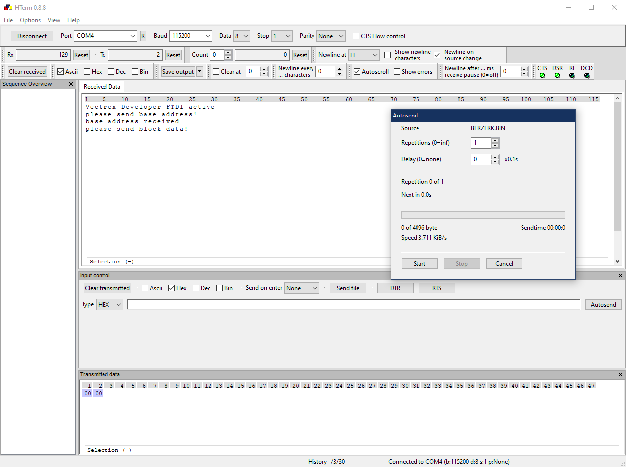
- On the PC side, the Vectrex
Developer is automatically registered as a
serial COM-port device, and a simple terminal
program is sufficient to communicate with the
Vectrex and to upload files.
- At the moment, I am using the HTerm
program. Copying files to the FRAMs this way is
actually a lot faster than with an EPROM burner.
Vectrex
Programming with the Vectrex Developer
- With the Vectrex Developer, binaries and games
that use the BIOS routines can effortlessly have
sizes up to ~48K. If the BIOS routines are not
needed, then the available size increases to ~56K.
Any portion of this can be used for RAM variables as
well as for code.
- Having all RAM instead of ROM also
allows for implementing fancy things like
self-modifying code.
- In combination with using the
Hitachi 6309 CPU, the Vectrex turns into a very
powerful upgraded system with
~56K RAM, and the extended instruction set and
increased performance of the 6309, which opens up
some very interesting programming possibilities and
a new universe to explore.
- The UART offers an easy means of
bidirectional communication with the outside
world that can be used in any Vectrex program.
For example, expensive computations could be
outsourced and handled by an external program
running on a laptop or PC which communicates its
results back to the Vectrex program. I am
thinking about trying this for fun with Kingslayer
Chess, with the Vectrex sending the chess
board configuration to some PC chess program
which then computes the moves and sends them
back.
- More experiments and reports will follow.
Hardware
Information and Development History
- The hardware needed for assembling the current
version of the board costs approximately 90 Euros.
- UART interface IC: FTDI FT245RNL
- FRAM IC: FM1808B-SG
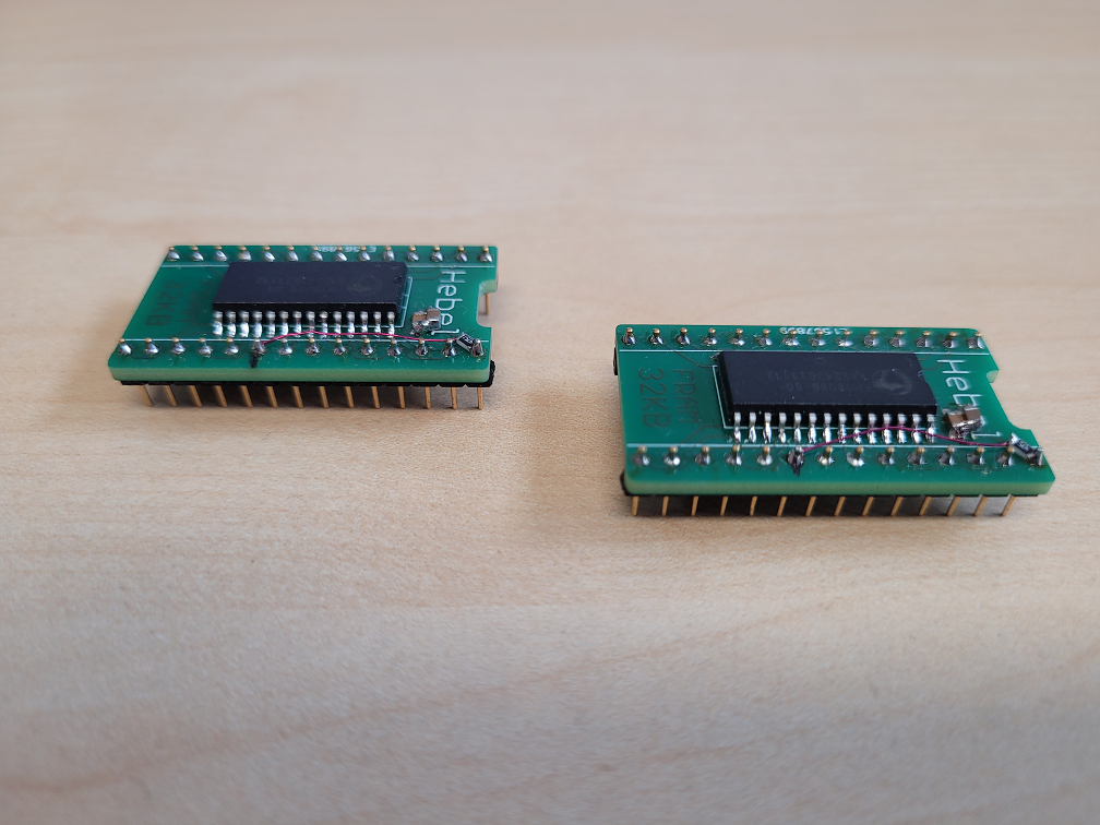
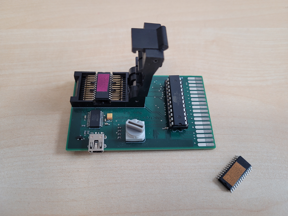
- The current version of the Vectrex Developer board
is actually our second physical prototype. Andreas
and I had lots of discussions, and our concept went
through many iterations. There was a first alpha
prototype which had no external cartridge connector.
Also, the lower FRAM was fixedly attached and
soldered to the board, and a ZIF-socket was used
only for the upper FRAM, see pictures below.
Credits
- Support: Timo Schwaab, Head of the
Electronics Workshop at Pforzheim University
- Hardware: Andreas Reber
- Software: Peer Johannsen
Contact
Latest modification on 11/15/2024,
17:00
|